Research
Structure of ChemPrint
ChemPrint reinvents semiconductors research. This CRC inaugurates the patterned growth of functional inorganic semiconductors from solution with atomic precision using molecular chemical control. The mild processing conditions are inherently energy-efficient and the additive approach materials-efficient, in stark contrast to the characteristics of traditional semiconductor manufacturing. According to our tenet, the ultimate degree of control achieved routinely in classical molecular chemistry can be advantageously transferred to interfacial reactions designed to grow semiconductor films with atomic precision. To this aim, we tailor molecular precursors, reaction environments, deposition procedures, and substrates in order to precision-engineer the reaction mechanisms, the elementary kinetics, the reversibility of individual steps, the interfacial energies, and the mobility of adspecies. Controlling these factors in mild conditions, potentially even at room temperature, shall achieve the highest possible degree of accuracy in positioning atoms or ions into regular structures. This strategy will then enable us to create original patterns and heterostructures along horizontal and vertical dimensions.
We aim for epitaxial material quality in various guises and corresponding functional quality, targeting semiconductors with either defect correction ability or intrinsic defect tolerance. The first funding period will establish quantitative design criteria for these currently imperfectly defined concepts. Accordingly, we will during the first four years gather data on three material families which cover a range of dimensionalities and chemical bonding types: heavier main group V (group 15) chalcogenides, halide perovskites, and transition metal dichalcogenides. The general insight gained will enable the consortium to choose the material focus for subsequent funding periods.
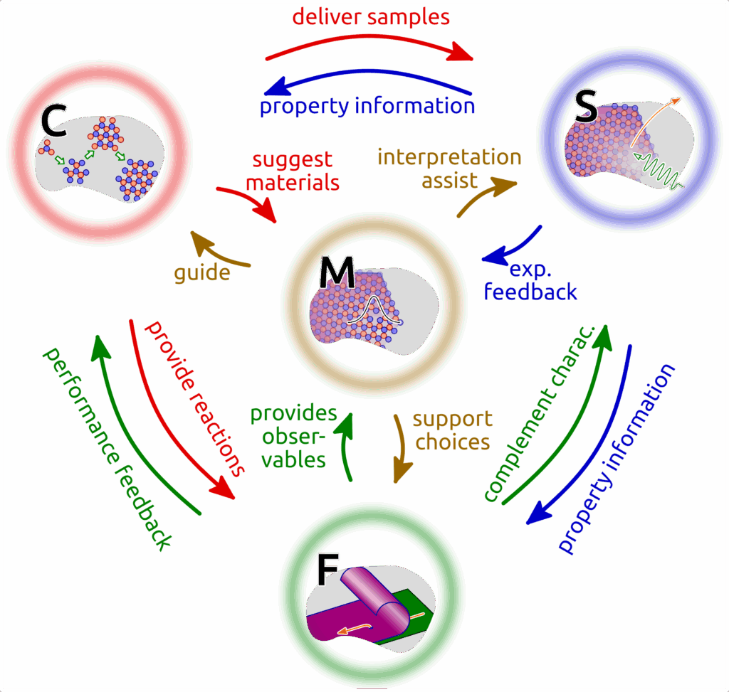
The six projects of Area C ― Surface chemistry and reactivity ― investigate nucleation, growth, and the mechanisms of individual reaction steps when material is added to the solid in individual atomic layers under molecular control. The precursors’ ligands, the solvent, surfactant additives, and preliminary surface treatments will be used as tools to adjust reactivity and selectivity in atomic layer deposition (ALD) from the gaseous and liquid phases. Novel molecular structures are designed and placed on the solid surface so as to enable for the definition of lateral patterns and vertical heterostructures. Kinetic and mechanistic information on these reactions will be provided via in-situ characterization methods including scanning electrochemical microscopy, vibrational spectroscopy, and nuclear magnetic resonance.
The materials created are investigated extensively in terms of their fundamental properties in Area S ― Structure and electronic properties. We establish their structure on length scales from atomic to nanometers and correlate them with the optoelectronic properties of thin-film semiconductors and their heterostructures. We apply a wide spectrum of methods, from imaging techniques to spectroscopic tools including local methods (scanning probe microscopy and electron microscopy) to address single defects and nucleation sites, but also ensemble averaging techniques: X-ray scattering, photoluminescence, Raman spectroscopy, and X-ray spectroscopy. The research driven by these five projects uncovers the structures, chemical identities, and physical properties of defects and interfaces.
The insight gained is then applied in Area F ― Functional properties and applications. Here, we decipher experimentally how opto-electronic properties translate into the dynamics of charge carriers and how heterostructures can be designed to take advantage of these dynamic properties . The photophysics are approached fundamentally on all timescales upwards of 100 fs via ultrafast one- and two-dimensional pump-probe spectroscopic methods, and the control of carriers exploited in devices (photodetectors, solar cells, transistors). Epitaxial control over large areas is required for consistent dynamic properties, with work dedicated to the engineering of individual epitaxial crystals, processing single-crystalline films and heterojunctions, and self-assembled monolayers as tools providing flexibility in heterostructure formation.
Area M ― Modeling and simulation ― enlightens experimental results on the mechanisms of surface reaction steps during nucleation and growth, the effects of transport in the fluid phase and at the interface, and the static and dynamic properties of charge carriers as they depend on structure, heterostructures and defects. Area M covers all time and length scales from fs to seconds and from Å to cm by combining an exhaustive set of methods, starting with modeling of excited states and the analysis of structural binding motifs using first-principles computations, continuing on the level of single nucleation seeds with molecular dynamics and for populations with Monte Carlo, and closing for film formation with phase-field approaches.
On a strategic level, the fundamental insight into low-temperature molecular reaction mechanisms at interfaces gained in ChemPrint will open up a new avenue in semiconductor processing. Suitable functional materials and semiconductor devices will be rendered accessible by approaches requiring low investments. Innovation by small economic actors will be possible again in information technology. This will reverse the economic trend in this sector, allowing it to revert to a more decentralized, more agile and nimble state, and potentially putting Germany at the spearhead of a flexible and robust semiconductor manufacturing industry.