Area F: Functional properties and applications
Area F the applies the insight gained in Area C and Area S to set the groundwork for functional devices. Since semiconductor devices inherently rely on the interaction of several materials phases and the precise definition of layers and heterostructures over samples of macroscopic size, the research in Area F addresses two broad goals:
- determine charge carrier transport properties and emissive recombination within ultrathin layers and charge transfer across the interface between semiconductor phases: F1 (Guldi), F3 (Brabec);
- optimie substrate and processing methods for the deposition and removal of high-quality functional layers and heterostructures: F3 (Brabec), F4 (Bachmann), F5 (Halik), F6 (Peters).
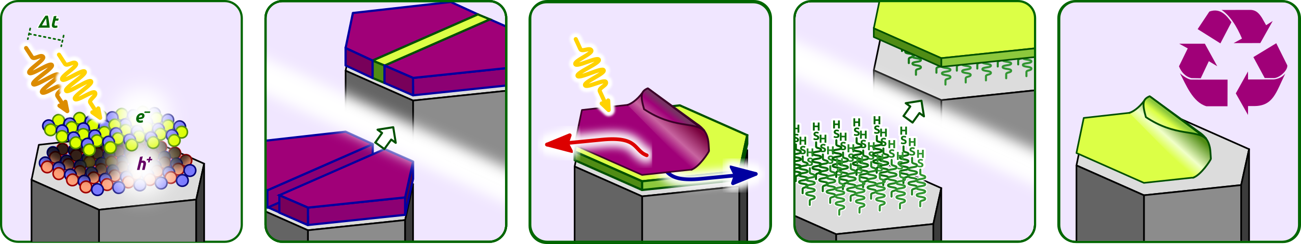
Project F1 (Guldi) is dedicated to investigating quasiparticles consisting of more than an electron and a hole (biexcitons, trions) in low-dimensional semiconductor phases and at their interfaces (with C1, C3, C4, S1, S2, S3, S4, S5, F3, F5, F6, M1, M2, M3). Charge transfer between two solids or between a solid and an adsorbed molecule may be associated with phenomena such as triplet fusion, which allow for fundamentally new ways to harvest solar energy. These phenomena will be characterized by one-dimensional and two-dimensional time-resolved ultrafast spectroscopy in the optical and vibrational regimes, as well as by Raman, Stark, and photoluminescence spectroscopies in the steady state.
Project leader: Prof. Dr. Dirk M. Guldi
Project F3 (Brabec) invents methods for the scalable printing of high-quality semiconductors by liquid-phase epitaxy. At the fundamental level, the project will determine how the particles within inks are generated and assembled upon evaporation of the solvent. Their interactions with each other laterally (with C6, S3, S5) and with the substrate underlying (with C1, C2, C3, C4, F6) will be controlled to determine epitaxial growth ― with modeling input from M1, M3, M4, M5. In terms of applications, the success of the deposition methods will be assessed by quantitative functional performance parameters with S4, F1.
Project leader: Prof. Dr. Christoph J. Brabec
Project F4 (Bachmann) takes solution ALD (from C1) to applications by demonstrating its use for depositing the light absorber layer in efficient solar cells. The project closes the ChemPrint cycle of innovation by combining atomic-level control in solution processing with performance quantifiers (with F3). It provides direct comparisons of processing techniques, between sALD and gALD on the one hand and between sALD and evaporation-based methods on the other hand (with F3), and demonstrate how the control of chemical bonds between deposit and substrate determines function (with S2, S3, S4, S5, F5, M2).
Project leader: Prof. Dr. Julien Bachmann
Project F5 (Halik) delivers methods for nucleation control and regiospecific growth on the basis of molecular self-assembled monolayers (SAMs). The molecular flexibility provided by SAMs will introduce some tolerance in epitaxial relationships and allow for the integration of high-quality semiconductor layers into devices. Structural design at the organic molecule level will enable the experimentalist to either transfer, decouple, or modify the structural information from a substrate crystal to the new layer deposited. SAMs will be provided to C1, C2, C3, C4 and F3, whereas F6 will benefit of characterization methods available in C5, S2, S3, S5, F1, F5 and molecular dynamics modeling from M3.
Project leader: Prof. Dr. rer. nat. Marcus Halik
Project F6 (Peters) addresses recycling of semiconductors in devices by exploiting novel sALD techniques (with C1, F4) to deposit and remove layers with atomic-level precision, exploiting tools developed in C3. The deposition and removal techniques are especially relevant for thin interface layers that are used for passivation or carrier selection. Additionally, such techniques will be highly relevant for all applications in which very thin layers of toxic or precious materials are used. We will explore the economic and sustainability implications by tracking material, energy and capital flows to establish the boundary conditions for such a process becoming industrially relevant.
Project leader: Dr. Ian Marius Peters